
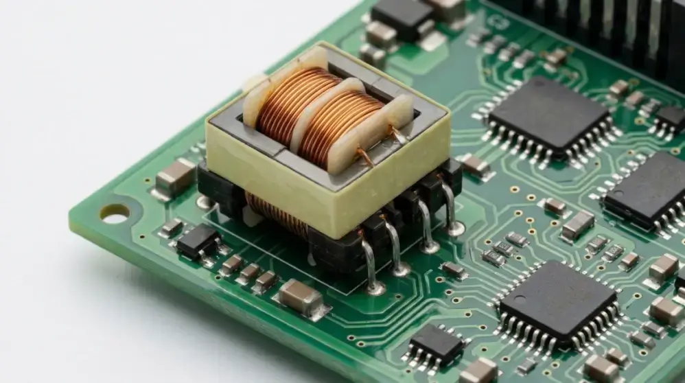
1.The GaN Revolution and the Need for Compact Power
Gallium Nitride (GaN) transistors have transformed the power supply industry by allowing switching frequencies to jump from 65kHz to well over 300kHz. While this drastically reduces the necessary size of magnetic components, traditional wire-wound transformers simply cannot keep up with these high frequencies without suffering severe AC copper losses. This is where the planar transformer becomes indispensable.
2. What is a Planar Transformer?
Unlike standard transformers that use round enameled wire wound around a plastic bobbin, a planar transformer utilizes flat copper traces embedded within a multi-layer Printed Circuit Board (PCB) or flat copper foils.
- Ultra-Low Profile: The flat design allows for power adapters that are incredibly thin, meeting the consumer demand for pocket-sized fast chargers.
- Excellent Thermal Dissipation: The flat surface area of the PCB and the core makes it much easier to attach heat sinks, preventing thermal runaway in compact enclosures.
3.Overcoming High-Frequency Challenges
Designing a planar transformer for a GaN charger involves precise engineering:
- Minimizing AC Resistance: At frequencies above 300kHz, the skin effect becomes a major issue. By using flat PCB traces, planar designs inherently reduce proximity effect and AC copper loss, ensuring higher overall efficiency.
- Optimizing the Magnetic Path: Because planar transformers operate at extreme frequencies, selecting the right magnetic core materials
is critical. High-frequency Mn-Zn ferrite grades with low Pv (Core Loss) are mandatory to prevent overheating.Controlling Energy Storage: Just like traditional flyback designs, planar transformers used in active clamp flyback (ACF) topologies require a highly precise transformer air gap to store energy and prevent premature magnetic saturation.

4. The Fringing Flux Challenge
While air gaps are necessary, they introduce a side effect known as fringing flux. Magnetic lines of force “bulge” outward as they cross the gap. If the copper windings are placed too close to this gap, the fringing flux cuts through the wire, inducing severe eddy currents and drastically increasing AC copper loss. A well-designed electronic transformer bobbin will keep the windings at a safe distance from the center gap.
5.Manufacturer’s Insight: Precision Grinding and AL Value
Calculating the gap is only half the battle; manufacturing it requires extreme precision. An error of just 0.05 mm in the gap length can result in a massive deviation in the AL value (Inductance Factor), leading to circuit instability. At our manufacturing facility, we utilize high-precision CNC grinding rather than relying solely on spacer tapes. Every gapped core undergoes rigorous LCR meter testing to ensure the final primary inductance matches the engineer’s exact specifications, guaranteeing consistent power delivery in mass production.
Conclusion
The transformer air gap is a micro-engineering marvel that dictates the energy storage and saturation limits of your power supply. By combining precise mathematical design with state-of-the-art CNC grinding capabilities, we deliver magnetic components that provide uncompromising stability for your most demanding topologies.